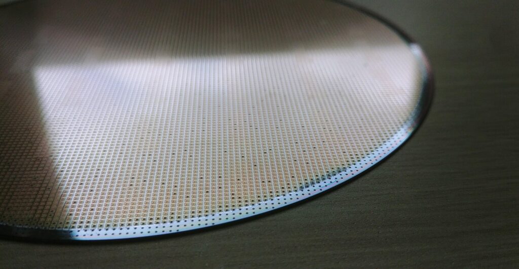
What Are Silicon Wafers?
Silicon is the primary material cost in semiconductor manufacturing. In the fast-moving world of semiconductor manufacturing, precision is everything. Silicon wafers—thin, circular slices of semiconductor material—serve as the foundation for microchips that power everything from smartphones to satellites. But what happens to wafers that don’t make the cut? Enter reclaimed silicon wafers: a sustainable, cost-effective solution gaining traction across multiple industries.
What Are Reclaimed Silicon Wafers?
Reclaimed silicon wafers are previously used wafers that have been restored through specialized cleaning, polishing, and testing processes. Rather than discarding them as scrap, manufacturers can reintroduce these wafers into the production cycle for specific, non-critical applications.
This approach not only reduces material waste but also lowers manufacturing costs and supports sustainability initiatives.
Common Uses for Reclaimed Silicon Wafers
1. Equipment Testing and Calibration
One of the most common uses for reclaimed wafers is in equipment testing. Semiconductor fabrication tools must be regularly calibrated and maintained to ensure optimal performance. Using brand-new prime wafers for these tasks would be unnecessarily expensive. Reclaimed wafers provide a cost-effective alternative for:
- Tool setup and alignment
- Process qualification
- Preventive maintenance routines
- Training purposes
Because these processes don’t require pristine wafers, reclaimed options are ideal.
2. Research and Development
R&D teams often run experimental processes, prototypes, and trials where perfect wafer quality isn’t essential. Reclaimed wafers allow engineers and researchers to:
- Test new materials or coatings
- Experiment with lithography processes
- Validate design changes
- Conduct failure analysis
Using reclaimed wafers reduces costs while still providing a realistic substrate for testing.
3. Solar Cell Manufacturing
Silicon is also the primary material used in photovoltaic (PV) solar cells. In some cases, reclaimed wafers can be repurposed for:
- Experimental solar cell designs
- Educational solar projects
- Low-cost photovoltaic applications
This reuse supports the renewable energy sector while minimizing raw material consumption.
4. MEMS and Sensor Prototyping
Microelectromechanical systems (MEMS) and sensor development often involve iterative testing and small production runs. Reclaimed wafers are commonly used for:
- Pressure sensor prototypes
- Accelerometers
- Microfluidic devices
- IoT sensor development
Since early-stage prototypes may not require prime-grade wafers, reclaimed options offer significant savings.
5. Educational and Training Applications
Universities, technical schools, and training facilities frequently use reclaimed wafers for:
- Semiconductor fabrication courses
- Cleanroom training exercises
- Engineering demonstrations
- Student research projects
These wafers provide hands-on experience without the high cost of new materials.
6. Optical and Specialty Applications
Some reclaimed wafers are repurposed for non-electronic uses, including:
- Optical components
- Decorative or architectural elements
- Precision mirrors or substrates
- Art and design projects
Their smooth, reflective surfaces and geometric precision make them attractive for creative and technical applications alike.
Environmental and Economic Benefits
Reduced Material Waste
Silicon wafer production is energy-intensive and resource-heavy. Reclaiming wafers:
- Diverts usable materials from landfills
- Reduces demand for raw silicon
- Lowers carbon footprint
Cost Savings
Reclaimed wafers can cost significantly less than new prime wafers, making them attractive for:
- High-volume testing environments
- Budget-conscious research labs
- Educational institutions
Support for Circular Manufacturing
By extending the life cycle of semiconductor materials, wafer reclaiming contributes to a circular economy model—where resources are reused, refurbished, and recycled instead of discarded.
How the Reclaim Process Works
At Semi-Metals, our reclaim process typically includes:
- Inspection: Identifying defects and assessing wafer condition.
- Stripping: Removing old films and contaminants.
- Polishing: Restoring surface smoothness and flatness.
- Cleaning: Eliminating particles and residues.
- Final Testing: Verifying thickness, flatness, and surface quality.
After this process is completed, the wafers are ready for reuse in appropriate applications.
The Future of Wafer Reclamation
As semiconductor demand continues to grow, so does the need for sustainable manufacturing practices. Wafer reclamation is expected to expand alongside:
- Increased environmental regulations
- Rising raw material costs
- Growth in R&D and emerging technologies
Companies that adopt reclaim strategies can reduce costs while supporting greener production methods.
Reclaimed silicon wafers demonstrate that high-tech industries can also embrace sustainability. From equipment testing to solar innovation, these restored materials provide practical, economical, and environmentally responsible solutions across a wide range of applications.
As technology evolves, reclaiming and reusing materials like silicon wafers will play an increasingly important role in shaping a more efficient and sustainable semiconductor ecosystem.
Contact Semi-Metals today at (636) 980-2755 or by email to learn how our reclaimed wafer solutions and help you optimize your business operations.